108年年會特邀演講來賓
學會於108年9月21日(星期六)於國立臺灣大學 工學院綜合大樓 國際演講廳203室 舉行第三十九屆年會暨會員大會,特別介紹二位年會特邀演講來賓。
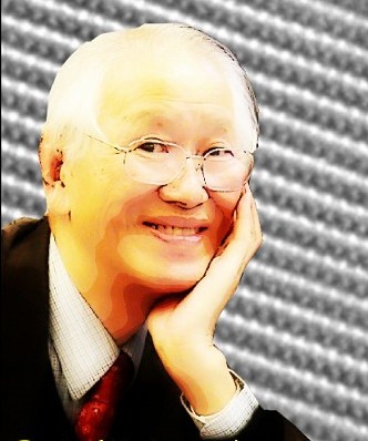
Professor Dr. Shiojiri, Makoto

- 演講題目:Some of our recent microscopy investigations
- 任職單位:Professor Emeritus of Kyoto Inst. Tech
- 演講摘要:
In the 39th Annual Meeting of Microscopy Society of Taiwan (2019), I’d like to talk about the following topics which relate to our recent studies of materials science and bio science.
I. Layer Growth, Coalescence and Layer Defects of Fine η Precipitates in 7050 Aluminium Alloy: Recently, we have published a paper on η precipitates in 7050 Aluminium Alloy. AA7050 (Al-Zn-Mg-Cu) is a heat treatable Al alloy with high toughness, strong mechanical strength, and good stress corrosion cracking resistance. It is a precipitate hardening alloy, used to build fuselage frames, wing skins and other aerospace structures.
II. Structure and Carbonization of Green Culms of Bambusa multiplex: Bambusa multiplex (蓬 莱竹) is a bamboo whose culm is straight with a height of 5~8 m and a diameter of 30~50 mm. The culm is very thick and heavy with small lumens, as represented by Japanese name ‘沈竹, a bamboo that sinks in the water’. The culms have been used for wood pulp and must be the useful material for cellulose nanofibers. Its charcoal would also be a promising new carbon material. Culms sampled and seasoned in Thailand were used in this experiments.
III. Nanoscale Nitride Epilayers Grown by Atomic Layer Annealing and Epitaxy at Low Temperature: AlN-based and GaN-based materials are widely used in electronic devices such as LED. High-quality ALN and GaN epilayers are conventionally grown by metal-organic chemical vapor deposition. However, they are grown at a very high temperature (> 900oC) with a large thickness up to ~600 nm on lattice mismatched substrates such as sapphire.
- 個人簡介:Professor Dr. Makoto Shiojiri was born in 1936 in Kyoto, Japan. He graduated from Kyoto University in 1959, and got M. Sc. from the same university in 1961, with his major in physics. After engaged in physical metallurgy at the Central Research Laboratory, Sumitomo Steel Co. Ltd., he was appointed an instructor at the Institute for Chemical Research, Kyoto University in 1962, and started his academic career, majoring in crystal and thin film physics and electron microscopy. He was conferred the D. Sc. from Kyoto University in 1967 for his studies on ‘Crystallization of amorphous films prepared by vacuum-evaporation'. He was promoted to an associate professor of physics at Kyoto Institute of Technology in 1966 and was appointed a full professor of the same institute in 1975. He stayed at the Faculty of Applied and Engineering Physics of Cornell University, U.S.A. and studied the ultrahigh vacuum electron microscopy, from 1971 to 1972.
At the end of March 1999, Dr. Shiojiri retired from Kyoto Institute of Technology and is a professor emeritus of the same institute. From June 1999 to March 2007, he was with graduate school in Kanazawa Medical University as a guest professor of anatomy. Now (2014~), he is also a fellow of Faculty of Engineering, University of Toyama. In November 2015, Professor Shiojiri was awarded the Order of the Sacred Treasure, Gold Rays with Neck Ribbon, from The Emperor of Japan.
His resume can be found in website: http://www009.upp.so-net.ne.jp/shiojiri/top.htm
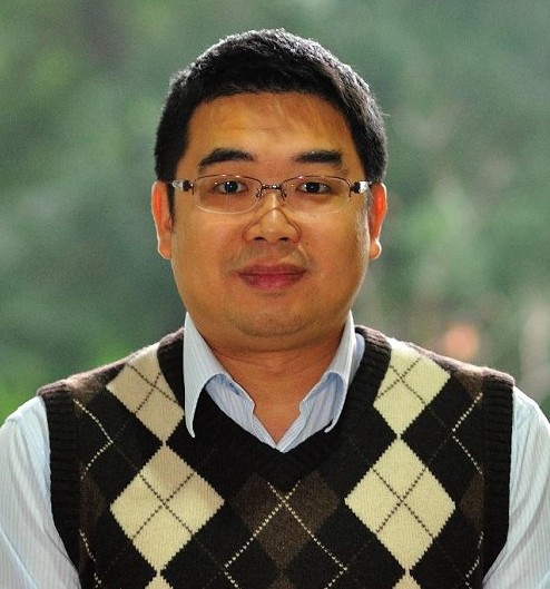
吳文偉 特聘教授 Dr. Wen-Wei Wu

- 演講題目:In-situ TEM investigation of dynamic evolution in nanostructures
- 任職單位:Department of Materials Science and Engineering, National Chiao Tung University, Hsinchu 300, Taiwan, ROC
- 演講摘要:In-situ TEM is a technique that allows a direct observation of dynamic properties in nanoscale. In situ investigation of the temperature induced phase transformation, structural and chemical evolution of nanocrystals is important for understanding the structure and stability of nanomaterials. As the technology advances, the scaling issue of nanodevices has attracted wide consideration, especially the exploration of atomic-scale structural dynamics. The appropriate utilization of the in-situ TEM will be beneficial in studying the fundamental mechanisms of dynamic reactions, switching behaviors and electrical properties of nanodevices. Therefore, we use in-situ TEM for direct observation of the dynamic evolution in nanomaterials and nanodevices, which is important for understanding their mechanisms and aiding to the practical aspect. Here, we present the most recent progress in observing dynamic processes in nanoscale by in-situ TEM.
- 現 職:國立交通大學材料科學與工程學系 特聘教授
- 學 歷:國立清華大學材料科學與工程所博士, 2003
- 經 歷:國立交通大學材料科學與工程學系教授, 2014
國立交通大學材料科學與工程學系 副教授, 2011~2014
國立交通大學材料科學與工程學系 助理教授, 2008~2011
國立清華大學材料科學與工程學系 博士後研究員, 2003~2008 - 專 長:電子顯微鏡、半導體材料、奈米光電材料、微電子材料與製程、材料顯微結構及缺陷分析、薄膜工程
- 簡 介: 吳文偉教授,國立清華大學材料科學與工程博士畢業(2003) ,2008年 2 月起任教於國立交通大學材料科學與工程學系。吳文偉教授研究領域為電子顯微鏡、半導體材料、奈米光電材料、微電子材料與製程。2008年與研究團隊發現銅晶體內部之奈米雙晶結構與晶界接合處可有效遲滯銅原子的電致遷移現象,對於積體電路製程技術的開發極具啟發作用,成果獲刊於國際頂尖期刊《Science》;隔年獲頒發「2009年 中央研究院年輕學者研究著作獎」。2014以「電阻式記憶體中傳導奈米燈絲之演變研究」獲得「第十二屆有庠科技奈米科技類論文獎」,為世界上首次成功用材料分析方法直接觀察電阻式記憶體透過氧化還原而導致電阻值轉換(switching)及結構動態變化完整過程的論文,對元件操作與物理模型提供良好的材料分析方法與驗證機制。此外,吳教授也榮獲「103年度 科技部吳大猷先生紀念獎」、「中國電機工程師學會優秀青年電機工程師獎」、「台灣真空學會年輕學者獎」、「台灣電子材料與元件協會傑出青年獎」以及「中國材料學會傑出年輕學者獎」等研究獎勵。吳教授專長為臨場穿透式電子顯微鏡研究,針對材料在通電、加熱、以及液態的環境下的物理現象與結構演變及成長動力學有許多創新與突破性的研究成果發表於頂尖期刊,獲得極大的迴響,因此更於107年榮獲「中國電機工程師學會傑出電機工程教授獎」以及「科技部傑出研究獎」。